Difference between revisions of "THz Waveform Synthesis"
From KAIST Quantum Computing Lab Wiki
Jump to navigationJump to search| Line 3: | Line 3: | ||
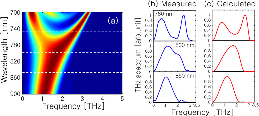
[[Image:Znte(wave(2).jpg|thumb|600px|left|alt=A cartoon centipede reads books and types on a laptop.|''Fig. 1. (a) Spectral bifurcation of generated terahertz waves from a 2-mm-thick ZnTe crystal, shown as a function of the pump laser wavelength. (b) Measured terahertz spectrums for three different pump laser wavelengths: 760, 800, and 850 nm.'' | [[Image:Znte(wave(2).jpg|thumb|600px|left|alt=A cartoon centipede reads books and types on a laptop.|''Fig. 1. (a) Spectral bifurcation of generated terahertz waves from a 2-mm-thick ZnTe crystal, shown as a function of the pump laser wavelength. (b) Measured terahertz spectrums for three different pump laser wavelengths: 760, 800, and 850 nm.'' | ||
]] | ]] | ||
| − | : | + | |
| + | [[Image:Silicon(spectra(5).jpg|thumb|650px|left|alt=A cartoon centipede reads books and types on a laptop.|''Fig. 2. A set of measured THz temporal shapes (a) and spectra (b), and calculated THz spectra (c) from different periods''<br>''of 500 um silicon and 100 um air layers via one-dimensioncal multilayer strutures.'']] | ||
Revision as of 03:10, 15 September 2009
- For a variety of applications such as telecommunications, signal processing, and material characterization, manipulating of the spatial and spectrum profile of THz pulse is often required. There have been many attempts to get specially intended THz spectrum. These attempts are mostly based on currently realizable optical design methods such as metamateriallms, photonic crystals, perforated metal sheets, generation crystal, multilayered structures, and so on.
- For a variety of applications such as telecommunications, signal processing, and material characterization, manipulating of the spatial and spectrum profile of THz pulse is often required. There have been many attempts to get specially intended THz spectrum. These attempts are mostly based on currently realizable optical design methods such as metamateriallms, photonic crystals, perforated metal sheets, generation crystal, multilayered structures, and so on.
