Difference between revisions of "Terahertz Materials and Science"
From KAIST Quantum Computing Lab Wiki
Jump to navigationJump to searchm |
m |
||
| (3 intermediate revisions by 2 users not shown) | |||
| Line 8: | Line 8: | ||
<br><br> | <br><br> | ||
<big>'''[[THz waveform synthesis]]'''</big> | <big>'''[[THz waveform synthesis]]'''</big> | ||
| − | * For a variety of applications such as telecommunications, signal processing, and material characterization, manipulating of the spatial and spectrum profile of THz pulse is often required. There have been many attempts to get specially intended THz spectrum. These attempts are mostly based on currently realizable optical design methods such as metamateriallms, photonic crystals, perforated metal sheets, generation crystal, multilayered structures, and so on.<br><br> | + | :* For a variety of applications such as telecommunications, signal processing, and material characterization, manipulating of the spatial and spectrum profile of THz pulse is often required. There have been many attempts to get specially intended THz spectrum. These attempts are mostly based on currently realizable optical design methods such as metamateriallms, photonic crystals, perforated metal sheets, generation crystal, multilayered structures, and so on.<br><br> |
| − | ::[[File:Znte(wave).jpg| | + | ::[[File:Znte(wave(2).jpg|center|600px]] |
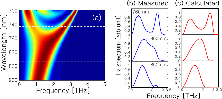
| − | <br>< | + | :::::::::''Fig. 1. (a) Spectral bifurcation of generated terahertz waves from a 2-mm-thick ZnTe crystal, shown as a function of the''<br>''pump laser wavelength. (b) Measured terahertz spectrums for three different pump laser wavelengths: 760, 800, and 850 nm.'' |
| − | + | <br><br>[[Image:Silicon(spectra(5).jpg|center|650px]] | |
| − | + | ::::::::''Fig. 2. A set of measured THz temporal shapes (a) and spectra (b), and calculated THz spectra (c) from different periods''<br>''of 500 um silicon and 100 um air layers via one-dimensioncal multilayer strutures.'' | |
| − | [[THz emission]] | + | <br><br><br> |
| + | <big>'''[[THz metamaterials]]'''</big> | ||
| + | |||
| + | |||
| + | <big>'''[[THz emission]]'''</big> | ||
Latest revision as of 08:11, 1 September 2009
What is Terahertz (THz)?
- THz fields : 0.1 ~ 10 THz (3 mm ~ 30 um)
- 1 THz = 1 ps = 0.3 mm = 33 cm-1 = 4.1 meV = 48 K.
- Unique physical phenomena in THz range : THz field penetrates non-metalic and non-polarizing materials(semiconductor, plastics, textiles).
- Main Application : spectroscopy, medical imaging, biology, and communications, etc.
- THz fields : 0.1 ~ 10 THz (3 mm ~ 30 um)
- The scientific and technological interest in the electromagnetic waves in the newly available frequency range of 0.1 ~ 10 THz, or terahertz (THz) wave, for short, has been gradually increasing, because of the potential uses of THz waves in a large variety of up-and-coming applications. To list a few, recent discoveries in THz science and technology found their applications in communications, material characterizations, biological and medical imaging, and precision spectroscopy of molecules. THz time-domain spectroscopy (THz-TDS) has become widely adopted, in particular, for the measurement of absorption and dispersion of materials in the THz frequency range. Moreover, THz pulse is extremely broadband in frequency and its usage beyond simple spectroscopy and imaging can be also easily found in its applications.
- For a variety of applications such as telecommunications, signal processing, and material characterization, manipulating of the spatial and spectrum profile of THz pulse is often required. There have been many attempts to get specially intended THz spectrum. These attempts are mostly based on currently realizable optical design methods such as metamateriallms, photonic crystals, perforated metal sheets, generation crystal, multilayered structures, and so on.
-
- Fig. 1. (a) Spectral bifurcation of generated terahertz waves from a 2-mm-thick ZnTe crystal, shown as a function of the
pump laser wavelength. (b) Measured terahertz spectrums for three different pump laser wavelengths: 760, 800, and 850 nm.
- Fig. 1. (a) Spectral bifurcation of generated terahertz waves from a 2-mm-thick ZnTe crystal, shown as a function of the
- For a variety of applications such as telecommunications, signal processing, and material characterization, manipulating of the spatial and spectrum profile of THz pulse is often required. There have been many attempts to get specially intended THz spectrum. These attempts are mostly based on currently realizable optical design methods such as metamateriallms, photonic crystals, perforated metal sheets, generation crystal, multilayered structures, and so on.
- Fig. 2. A set of measured THz temporal shapes (a) and spectra (b), and calculated THz spectra (c) from different periods
of 500 um silicon and 100 um air layers via one-dimensioncal multilayer strutures.
- Fig. 2. A set of measured THz temporal shapes (a) and spectra (b), and calculated THz spectra (c) from different periods
